Showing posts with label Standard Cell Library. Show all posts

30 August

DeCap Cells in Physical Design | Use of Decap Cells in PD

Decap cells are basically a charge storing device made of the capacitors and used to support the instant current requirement in the power delivery network. There are various reasons for the instant large current requirement in the circuit and if there are no adequate measures have taken to handle this requirement, power droop or ground bounce may occur. These power droop or ground bounce will affect the constant power supply and ultimately the delay of standard cells may get affected. To support the power delivery network from such sudden power requirements, decap cells are inserted throughout the design. In this article, we will discuss the structure and layout of decap cells, need of using decap cell and placement of decap cells.

Schematic and layout of Decap cell:

There could be various ways to make capacitors out of MOS transistors but the must widely used structure is shown in the figure-1. 


Figure-1: MOS Capacitances and Decap cell schematics

Figure-1(a) shows the various capacitances inside the MOS transistor and it if we connect the source, drain and body terminal together then all these capacitance will configured as a parallel capacitance as shown in figure-1(b) and a single equivalent capacitance as shown in figure-1(c). Figure-1(d) shows a decap capacitor schematic using a pMOS and an nMOS transistor. From this schematic, we can say that the capacitance due to nMOS and pMOS will be in parallel and get added to form a big capacitor. Figure-2 shows the layout of a simplest decap cell.


Figure-2: Layout a decap capacitor 

Source and drain of pMOS transistor shorted together and connected to VDD and the Gate is connected to VSS. Similarly, the source and drain of the nMOS transistor are connected to the VSS and gate is connected to VDD.


Use of  Decap cell:

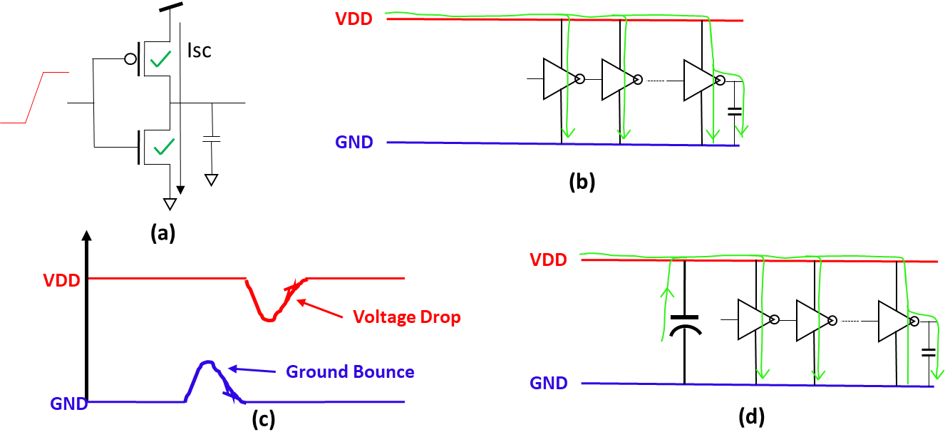
In the operation of CMOS logic, there is a region of input transition where both the nMOS and pMOS is conducting together as shown in figure-2(a). A large short circuit current Isc will flow for that instant. If a large number of such cells are placed together and switching together, a large current will be required as shown in figure-2(b). This large current requirement may drop the VDD or may increase the ground voltage which is called voltage droop or groud bounce as shown in figure-2(c).

Figure-2: Need of Decap cell

Voltage droop or ground bounce may result in the change in the delay of connected standard cells. As the delay is proportional to the supply voltage. Change in delay may further affect the timing of design and if the supply voltage drop is high, the functionality of the standard cell may get affected. So to support the power delivery, we add the decap cells. Decap cells work as charge reservoirs and support the power delivery network and make it robust as shown in the figure-2(d). 

Placement of  Decap cell:

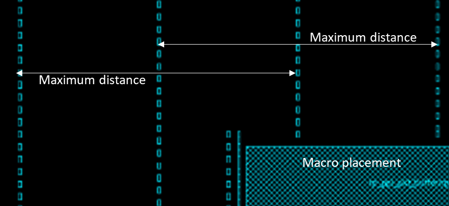
Decap cells are placed generally after the power planning and before the standard cell placement, that is in the pre-placement stage. These cells are placed uniformly throughout the design in this stage. Decap cells can also be placed in the post route stage also if required. 

The only problem with decap cells is that these are leaky and increases the leakage power of design, so must be used judiciously. 


Thank you.

29 August

Well Tap Cells in Physical Design

Well tap cells (or Tap cells) are used to prevent the latch-up issue in the CMOS design. Well tap cells connect the nwell to VDD and p-substrate to VSS in order to prevent the latch-up issue. There is no logical function in well tap cell rather than proving a taping to nwell and p-substrate therefore well tap cell is called a physical-only cell. In this article, we will discuss the structure of well tap cell, the requirement of well tap cell and how to place them in the physical design flow.

Well Tap Cell:

Well tap cells having no logical functions, it has only two connections.

  • nwell to the power supply (VDD)
  • p-substrate to the ground (VSS)

A typical structure of well tap layout has shown in figure-1. Well tap cell has no input and output pins, therefore it is called a physical-only cell.

Figure-1: Layout of well tap cell

Why Well Tap Cell:

Early days there was no concept of well tap cell, Standard cells were designed in such a way that each standard cell had nwell to VDD and p-substrate to VSS connection within the standard cell. But such a standard cell design had consumed more area and to save the area, later a concept of Tapless cell has evolved. In a tapless cell, there are no well taping inside the standard cell, well taping is provided by a separate standard cell which is called a well tap cell. So well tap cell is a part of a tapless standard cell library. Figure-2 shows the structure of a traditional standard cell and a tapless standard cell.

Figure-2: Traditional and Tapless standard cell structure

Well tap cells are used to prevent the latch-up issue in design. how it prevent, has been explained in the article "latch-up prevention in CMOS" in this blog. 

Placement of  Well Tap Cells:

Well tap cells are placed after the macro placement and power rail creation. This stage is called the pre-placement stage. Well tap cells are placed in a regular interval in each row of placement. The maximum distance between the well tap cells must be as per the DRC rule of that particular technology library. A typical placement of well tap cells is shown in figure-3. 


Figure-3: Well tap cell placement

Well tap cells are generally placed in a straight column in the alternate row as shown in figure and such a pattern is called checkerboard pattern to provide maximum coverage for well tap. If a macro comes in the path of vertical columns, then the placement of vertical column shifted alongside macro as shown in the figure. 

This placement is performed using the PnR tool command. For ICC and Innovus tool following command have used to place the well tap cells.


For Innovus tool:

set_well_tap_mode -rule <> -bottom_tap_cell <cellName> -top_cell_name <cellName> -cell <> 

addWellTap  -cell <cellName> -cellInterval <maxGap> -prefix <prefixName> -checkerBoard -fixedGap

verifyWellTap -report <reportName>

For more details refer UG of Innovus tool.


For ICC tool:

add_tap_cell_array -ignore_soft_blockage true -master_cell_name $tapCell –distance $tapPitch -connect_power_name VDD -connect_ground_name VSS -respect_keepout -pattern stagger_every_other_row -tap_cell_identifier WELLTAP 


Thank you!


28 August

Standard Cell Library for ASIC Design

Standard cell library is an integral part of ASIC design flow and it helps to reduce the design time drastically. Standard cells used in the ASIC design is a part of a standard cell library along with some other file sets. In this article, we will discuss the important content inside the standard cell library and its uses.

Standard Cell Library:

Standard cell library is a collection of well defined and pre-characterized logic cells with multi-drive strength and multi-threshold voltage cells in the form of a predefined standard cell layout. It also contains a number of physical only cells and a set of library files required by Place and Route (PnR) tool for automatic placement and routing (APR).

Pre-characterization: 

Before including a standard cell into standard cell library, the cells are gone through schematic design, simulations followed by Symbol creation, layout design (as per standard cells layout rules), physical verifications, abstraction, extraction and characterization. So the cells available in standard cell library are free from any DRC violations, well-characterized and suitable for PnR tool for automatic placement and routing.

Multi-drive strength cells: 

A low drive strength cell will require less power and area but having more delay and more transition time whereas a high drive strength cell can drive a larger number of cells and having a fast transition. So as per the requirement, a PnR design engineer chooses the drive strength of cells to optimize the area, power and performance.

Multi-Vt cells: 

A low threshold voltage (LVT) cell will have a lesser delay but higher leakage power as compared to a high threshold voltage (HVT) cell. So as per the requirement of timing and power a PnR engineer uses HVT and LVT cell to balance the power and timing of the design. There is no difference in the area on multi-Vt cells. A modern standard cell library contains generally ULVT, LVT, SVT, HVT types of cells in which Vt is in increasing order.

Physical only cells: 

In physical design, We need to add a variety to standard cells to mitigate various effects and manufacturing issues. These cells do not have any logical functions. For example to overcome the latch-up issue we need to add well tap cells. Decap cells, endcap cells, antenna cells and filler cells are the example of such cells.  

In the next section, we will discuss various cells collection and standard cells library and the set of important files.


Cell Collections:

In general, a standard cell library contains the following types of cell:

  • All basic and universal gates (like AND, OR, NOT, NAND, NOR, XOR etc)
  • Complex gates (like MUX, HA, FA, Comparators, AOI, OAI etc)
  • Clock tree cells (like Clock buffers, clock inverters, ICG cells etc)
  • Flip flops and latches
  • Delay cells 
  • Physical only cells
  • Scannable Flip flops

File Collections:

Apart from the standard cells, Standard cell library is delivered with a collection of files which contains all the information required to auto place and route. These files are mainly:

    • LIB files (.lib) 
    • LEF files (.lef)
    • Netlist file (.v )
    • GDS file (.gds)
    • SPICE Netlist (.sp)
    • Model file (.m)

All the format of files mentioned here with the reference of the Cadence tool. Some files format is different in the Synopsys tool but the information inside the file is the same. Brief information of these files is given below. Detailed information of all these files can be found in the "File in VLSI" section of this blog. 

Timing library (LIB or DB) files are generated during the characterization of cells. Library files contain cell delay, power and area information. Physical library (LEF) file is an abstract view of the layout of the cells. LEF file contains the information of cell boundary, Pins inside the cell, location, direction, and metal layer of each pin. Netlist file is a Verilog file of the standard cell which defines the functionality of a cell. GDS file is the layout of the standard cell. SPICE netlist is the netlist of cell in SPICE format is used for simulation. Model file contains the various design parameters of the cell required for SPICE simulation. 


Thank you.

18 May

Standard Cells in ASIC Design | Standard Cells in VLSI

Standard cells are well defined and pre-characterized cells used in ASIC (Application Specific Integrated Circuit) Design flow as basic building blocks. All these cells are equal in height and can easily fit into the standard cell row. Standards cells are highly reusable and save lots of ASIC design time.

Standard Cell Layout

All the Standard cells are in equal in height and varying width. Main characteristics of a standard cell have been explained with the help of the following figure.


   Figure-1: Standard Cell layout style

At the top of the standard cell, there is VDD rail and bottom there is a VSS rail. Both the Power rails are drawn in the Metal-1 layer. In between the VDD rail and VSS rail there are three main regions, a nwell region, a gap of nwell and pwell and pwell region. nwell region is near to the VDD rail and pwell region is near the VSS rail. pMOS transistors are build inside the nwell, so all the pMOS transistors are in the top half of the cell and similarly, all nMOS are in the bottom half of the standard cell.

Layout of a schematic can be drawn in various ways. For example layout of a NAND gate can be drawn in following two different styles. 
 Figure-2: Schematic of a NAND gate

 Figure-3: Layout of a NAND gate

 Figure-4: Layout of a NAND gate

Figure-2 is showing the schematic of a NAND gate and figure-3 and figure-4  showing two different layouts of the schematic shown in the figure. In figure 3 both the nMOS are in not the same level, they are stacked but in the layout of figure 4 all nMOS are in one level and all pMOS are at one level. And in figure-3 gates are drawn horizontal and not common in nMOS and pMOS. But in figure-4, all the poly gates are drawn vertical and common to nMOS and pMOS both. 


There are many reasons f0r preferring a layout style like in figure-4. Some of them are:

1. Save Design Area: Both the nwell and pwell are in the same level for all the standard cell, so they can easily abut and make a common well which saves lots of areas.
2. Easy placement for APR tool: All the standard cells have the same height and easily can be fit into the standard cell row so make it easy for APR (Automatic Place and Route) to place them. They also have power rails in the same location for all the standard cells, so power rails can also be abutted easily. 
3. Easy to route: All the pins of standard cells are in the intersection of horizontal and vertical tracks, So it becomes easy to route them by the APR tool

Tracks in standard cells:

Track can be defined as a line on which metal layers are drawn. A track means one M1 Pitch. Height of Standard cell is generally measured in term of no. of tracks inside it. like a 6T standard cell means that the height of the standard cell is 6 Track of M1. An example of 13T standard cell is given below in figure-5.

Figure-5: A 13T height standard cell

In the above example, the height of one track is 190 nm. So total height of cell is  13T = 2470 nm (13 x 190) and width is 5T = 950 nm (5 x 190).    

Various heights standard cell library:

Generally, there are various sets of standard cell library having different track size of standard cells. Depending on the use of ASIC, track height a standard library has selected. There are generally three sets of standard cell library characterized as small transistor standard cell, large transistors standard cell and medium transistor standard cell. An example for 6T, 12T and 9T size standard cells are shown below.


Figure-6: Various height's of standard cell 

Small transistor standard cells are used for high-density design and these cells having low power consumption. Large transistors standard cells large area but having very good performance. Medium transistors standard cells have a balance between large transistors and small transistors. So there is a tradeoff between area/power vs performance. A comparison has been shown below in figure-7.

Figure-7: Tradeoff between performance and area for various heights standard cell


Various applications of these cells are as bellow.

  • Small transistor cells (6T Cells)
    • Minimum area and low power
    • Mobile applications
    • Ultra-low-power applications
    • Embedded microcontroller
  • Large transistors cells (12T Cells)
    • Large area
    • High performance and speed
    • High-speed computing 
    •  Critical blocks
  • Medium transistors cells (9T Cells)
    • Balance area and performance
    • General Computing
    • GPU
    • General-purpose circuit

Thank you!