30 August

Spare Cells in Physical Design

Once a chip is fabricated and if any functionality issue is found in the chip or some functionality enhancement is required in the next fabrication. This might be a very challenging task without spare cells. But with the help of pre-placed spare cells, these changes can be done very easily. In this article, we will discuss the spare cells in physical design.  

Spare cells:

Spare cells generally consist of a group of standard cells mainly inverter, buffer, nand, nor, and, or, exor, mux, flip flops and maybe some specially designed configurable spare cells. Ideally, spare cells do not perform any logical operation in the design and act as a filler cell only. A group of spare cells is shown below. 


The inputs of spare cells are tied either VDD or VSS through the tie cell and the output is left floating. Input can not be left floating as a floating input will be prone to get affected by noise and this could result in unnecessary switching in space cells which leads to extra power dissipation.


Use of Spare cells:

Spare cells enable us to modify/improve the functionality of a chip with minimal changes in the mask. We can use already placed spare cells from the nearby location and just need to modify the metal interconnect. There is no need to make any changes in the base layers. Using metal ECO we can modify the interconnect metal connection and make use of spare cells. We only need to change some metal mask, not the base layer masks.

For example, suppose in the above circuit we need to replace the last OR gate in the middle part of a circuit with an EXOR or an AND gate, we can reconnect the spare cell placed near this with metal ECO only.

Placement of Spare cells:

Spare cells can be added either by the netlist or by PnR tool command (or GUI too). In Physical design, we prefer to add the spare cells using tool command. These cells are added before the placement of standard cells throughout the design. The way of adding spare cells for Innovus and ICC tool has been explained below.

Innovus tool:


ICC tool:


Advantage and disadvantage of Spare cells:

Advantage:

Reusability: 

There is only change in some metal and via masks, so base layers mask can be reused in chip fabrication.

Flexibility: 

Small changes can be done in the design very easily.

Cost and Time saving: 

We need only a few interconnect mask for a new design, which save lots of manufacturing cost for new chip fabrication. And using metal ECO we do not need to run full design cycle and therefore save design time.

Disadvantage:

Leakage Power: 

Spare cells increase the leakage power dissipation in the design.

Area: 

Spare cells cost extra area overhead in the design.


Thank You.


DeCap Cells in Physical Design | Use of Decap Cells in PD

Decap cells are basically a charge storing device made of the capacitors and used to support the instant current requirement in the power delivery network. There are various reasons for the instant large current requirement in the circuit and if there are no adequate measures have taken to handle this requirement, power droop or ground bounce may occur. These power droop or ground bounce will affect the constant power supply and ultimately the delay of standard cells may get affected. To support the power delivery network from such sudden power requirements, decap cells are inserted throughout the design. In this article, we will discuss the structure and layout of decap cells, need of using decap cell and placement of decap cells.

Schematic and layout of Decap cell:

There could be various ways to make capacitors out of MOS transistors but the must widely used structure is shown in the figure-1. 


Figure-1: MOS Capacitances and Decap cell schematics

Figure-1(a) shows the various capacitances inside the MOS transistor and it if we connect the source, drain and body terminal together then all these capacitance will configured as a parallel capacitance as shown in figure-1(b) and a single equivalent capacitance as shown in figure-1(c). Figure-1(d) shows a decap capacitor schematic using a pMOS and an nMOS transistor. From this schematic, we can say that the capacitance due to nMOS and pMOS will be in parallel and get added to form a big capacitor. Figure-2 shows the layout of a simplest decap cell.


Figure-2: Layout a decap capacitor 

Source and drain of pMOS transistor shorted together and connected to VDD and the Gate is connected to VSS. Similarly, the source and drain of the nMOS transistor are connected to the VSS and gate is connected to VDD.


Use of  Decap cell:

In the operation of CMOS logic, there is a region of input transition where both the nMOS and pMOS is conducting together as shown in figure-2(a). A large short circuit current Isc will flow for that instant. If a large number of such cells are placed together and switching together, a large current will be required as shown in figure-2(b). This large current requirement may drop the VDD or may increase the ground voltage which is called voltage droop or groud bounce as shown in figure-2(c).

Figure-2: Need of Decap cell

Voltage droop or ground bounce may result in the change in the delay of connected standard cells. As the delay is proportional to the supply voltage. Change in delay may further affect the timing of design and if the supply voltage drop is high, the functionality of the standard cell may get affected. So to support the power delivery, we add the decap cells. Decap cells work as charge reservoirs and support the power delivery network and make it robust as shown in the figure-2(d). 

Placement of  Decap cell:

Decap cells are placed generally after the power planning and before the standard cell placement, that is in the pre-placement stage. These cells are placed uniformly throughout the design in this stage. Decap cells can also be placed in the post route stage also if required. 

The only problem with decap cells is that these are leaky and increases the leakage power of design, so must be used judiciously. 


Thank you.

End Cap Cells in VLSI | Boundary Cells in VLSI

There are high chances to get damaged the gate of standard cells placed at the boundary during the manufacturing of chip. To prevent such damages at the boundary we have a special kind of cell in the standard cell library is called end cap cell or boundary cell. Boundary cell not only protects the gate damage at the boundary, but it also serves many other purposes. In this article, we will discuss the need for boundary cell placement, the structure and placement of boundary cells.

Where to place End Cap / Boundary Cells:

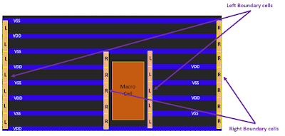
The end cap cell or boundary cell is placed at both the ends of each placement row to terminate the row. It has also been placed at the top and bottom row at the block level to make integration with other blocks. Some standard cell library has also corner end cap cells to place the corner of the block. Boundary cells have fixed attribute, therefore these cells can not be moved during the optimization. A typical placement of end cap cells at the end of the row has shown in figure-1. 

Figure-1: Placement of end cap cell at the end of rows

Why need to place End Cap / Boundary Cell?

The end cap cells are placed in the design because of the following reasons:

  • To protect the gate of a standard cell placed near the boundary from damage during manufacturing.
  • To avoid the base layer DRC (Nwell and Implant layer) at the boundary.
  • To make the proper alignment with the other block.
  • Some standard cell library has end cap cell which serve as decap cell also.

Layout of end cap / boundary cell:

The boundary cell is a physical-only cell, has no logical functions and therefore these cells are not a part of the netlist.  Boundary cells have mainly Nwell layer, implant layers, and dummy poly layer and metal rails as shown in the figure-2. 


How to place:

Boundary cells are placed just after the macro placement and site row creation. Boundary cell is placed before the placement of standard cells and therefore it is called a pre-placed cell. End cap cells cab be added using GUI interface or through the tool commands. Commands to add the endcap cells in Innovus and ICC tools have given below.

For Innovus tool:

setEndCapMode -reset
setEndCapMode -rightEdge <CellName> -leftEdge <CellName> -topEdge <CellName> -bottomEdge <CellName>  -rightTopEdge <CellName> -rightBottomEdge <CellName> -leftTopCorner <CellName> -leftBottomCorner <CellName>
addEndCap -prefix <name>
verifyEndCap -report <reportName>

For ICC tool:

insert_boundary_cell
 
For details of these commands and related switches refer to the tool's command man page.

Thank you.


29 August

Well Tap Cells in Physical Design

Well tap cells (or Tap cells) are used to prevent the latch-up issue in the CMOS design. Well tap cells connect the nwell to VDD and p-substrate to VSS in order to prevent the latch-up issue. There is no logical function in well tap cell rather than proving a taping to nwell and p-substrate therefore well tap cell is called a physical-only cell. In this article, we will discuss the structure of well tap cell, the requirement of well tap cell and how to place them in the physical design flow.

Well Tap Cell:

Well tap cells having no logical functions, it has only two connections.

  • nwell to the power supply (VDD)
  • p-substrate to the ground (VSS)

A typical structure of well tap layout has shown in figure-1. Well tap cell has no input and output pins, therefore it is called a physical-only cell.

Figure-1: Layout of well tap cell

Why Well Tap Cell:

Early days there was no concept of well tap cell, Standard cells were designed in such a way that each standard cell had nwell to VDD and p-substrate to VSS connection within the standard cell. But such a standard cell design had consumed more area and to save the area, later a concept of Tapless cell has evolved. In a tapless cell, there are no well taping inside the standard cell, well taping is provided by a separate standard cell which is called a well tap cell. So well tap cell is a part of a tapless standard cell library. Figure-2 shows the structure of a traditional standard cell and a tapless standard cell.

Figure-2: Traditional and Tapless standard cell structure

Well tap cells are used to prevent the latch-up issue in design. how it prevent, has been explained in the article "latch-up prevention in CMOS" in this blog. 

Placement of  Well Tap Cells:

Well tap cells are placed after the macro placement and power rail creation. This stage is called the pre-placement stage. Well tap cells are placed in a regular interval in each row of placement. The maximum distance between the well tap cells must be as per the DRC rule of that particular technology library. A typical placement of well tap cells is shown in figure-3. 


Figure-3: Well tap cell placement

Well tap cells are generally placed in a straight column in the alternate row as shown in figure and such a pattern is called checkerboard pattern to provide maximum coverage for well tap. If a macro comes in the path of vertical columns, then the placement of vertical column shifted alongside macro as shown in the figure. 

This placement is performed using the PnR tool command. For ICC and Innovus tool following command have used to place the well tap cells.


For Innovus tool:

set_well_tap_mode -rule <> -bottom_tap_cell <cellName> -top_cell_name <cellName> -cell <> 

addWellTap  -cell <cellName> -cellInterval <maxGap> -prefix <prefixName> -checkerBoard -fixedGap

verifyWellTap -report <reportName>

For more details refer UG of Innovus tool.


For ICC tool:

add_tap_cell_array -ignore_soft_blockage true -master_cell_name $tapCell –distance $tapPitch -connect_power_name VDD -connect_ground_name VSS -respect_keepout -pattern stagger_every_other_row -tap_cell_identifier WELLTAP 


Thank you!


28 August

Standard Cell Library for ASIC Design

Standard cell library is an integral part of ASIC design flow and it helps to reduce the design time drastically. Standard cells used in the ASIC design is a part of a standard cell library along with some other file sets. In this article, we will discuss the important content inside the standard cell library and its uses.

Standard Cell Library:

Standard cell library is a collection of well defined and pre-characterized logic cells with multi-drive strength and multi-threshold voltage cells in the form of a predefined standard cell layout. It also contains a number of physical only cells and a set of library files required by Place and Route (PnR) tool for automatic placement and routing (APR).

Pre-characterization: 

Before including a standard cell into standard cell library, the cells are gone through schematic design, simulations followed by Symbol creation, layout design (as per standard cells layout rules), physical verifications, abstraction, extraction and characterization. So the cells available in standard cell library are free from any DRC violations, well-characterized and suitable for PnR tool for automatic placement and routing.

Multi-drive strength cells: 

A low drive strength cell will require less power and area but having more delay and more transition time whereas a high drive strength cell can drive a larger number of cells and having a fast transition. So as per the requirement, a PnR design engineer chooses the drive strength of cells to optimize the area, power and performance.

Multi-Vt cells: 

A low threshold voltage (LVT) cell will have a lesser delay but higher leakage power as compared to a high threshold voltage (HVT) cell. So as per the requirement of timing and power a PnR engineer uses HVT and LVT cell to balance the power and timing of the design. There is no difference in the area on multi-Vt cells. A modern standard cell library contains generally ULVT, LVT, SVT, HVT types of cells in which Vt is in increasing order.

Physical only cells: 

In physical design, We need to add a variety to standard cells to mitigate various effects and manufacturing issues. These cells do not have any logical functions. For example to overcome the latch-up issue we need to add well tap cells. Decap cells, endcap cells, antenna cells and filler cells are the example of such cells.  

In the next section, we will discuss various cells collection and standard cells library and the set of important files.


Cell Collections:

In general, a standard cell library contains the following types of cell:

  • All basic and universal gates (like AND, OR, NOT, NAND, NOR, XOR etc)
  • Complex gates (like MUX, HA, FA, Comparators, AOI, OAI etc)
  • Clock tree cells (like Clock buffers, clock inverters, ICG cells etc)
  • Flip flops and latches
  • Delay cells 
  • Physical only cells
  • Scannable Flip flops

File Collections:

Apart from the standard cells, Standard cell library is delivered with a collection of files which contains all the information required to auto place and route. These files are mainly:

    • LIB files (.lib) 
    • LEF files (.lef)
    • Netlist file (.v )
    • GDS file (.gds)
    • SPICE Netlist (.sp)
    • Model file (.m)

All the format of files mentioned here with the reference of the Cadence tool. Some files format is different in the Synopsys tool but the information inside the file is the same. Brief information of these files is given below. Detailed information of all these files can be found in the "File in VLSI" section of this blog. 

Timing library (LIB or DB) files are generated during the characterization of cells. Library files contain cell delay, power and area information. Physical library (LEF) file is an abstract view of the layout of the cells. LEF file contains the information of cell boundary, Pins inside the cell, location, direction, and metal layer of each pin. Netlist file is a Verilog file of the standard cell which defines the functionality of a cell. GDS file is the layout of the standard cell. SPICE netlist is the netlist of cell in SPICE format is used for simulation. Model file contains the various design parameters of the cell required for SPICE simulation. 


Thank you.

27 August

Electromigration Effect in VLSI

Electromigration is an important issue especially in lower technology node where the cross-sectional area of metal interconnects is very less. In this article, we will discuss the phenomenon of electromigration, the effects of electromigration and the ways to prevent the electromigration issue. 

Electromigration:

When a high current density passes through a metal interconnect, the momentum of current-carrying electrons may get transferred to the metal ions during the collision between them. Due to the momentum transfer, the metal ions may get drifted in the direction of motion of electrons. Such drift of metal ions from its original position is called the electromigration effect. 

Current density J is defined as the current following per unit cross-section area. 

                       J = I/A

                            Where I is the current and A is the cross-section of the area of interconnect.

As the technology node shrinks, Cross-sectional area of the metal interconnects also shrinks and the current density increases in great extent in the lower node. Electromigration has been a problem since 90 nm technology node or even earlier but it gets worse in lower technology node 28nm or lower node.

Electromigration Phenomenon:


Figure-1: Electromigration phenomenon


Figure-1 shows the phenomenon of electromigration effect. A potential difference is applied across a metal interconnect which setups an electric field from anode side to cathode side as shown. This electric field causes to move the electron in the opposite direction of the electric field. This momentum of electron cause flow of current in the electron. These moving electrons have momentum and when it collides with the metal ions the metal ions feel two forces in the opposite direction as shown in the figure. One force and due to electric field and other is due to strike of electrons wind. If the current density is high the force due to electron wind is greater than the force due to the electric field.

Depending on the current density, the subjected metal ion started drifting in the opposite direction of the electric field.  If the current density is high, the interconnect may get affected of EM instantly or some times the effect may come after months/years of operation depending on current density. So the reliability of ASIC will depend upon this EM effect. 

Mean Time To Failure (MTTF) is an indication of the life span of an integrated circuit. MTTF is calculated using Black's equation as bellow.

Where A = Cross-Section area
            J = Current density
            N = Scaling factor (normally set to 2)
            Ea = Activation energy
            K = Boltzmann's constant
            T = Temperature in Kelvin 

Effects of EM:

Once the metal ions get started to shifting from its original position, these will create problem in the interconnect. It could result in an excess of ions accumulation in a particular location of deficient of ions. So either Hillocks or Void could occur in the metal interconnect. 


Figure-2: Hillock and Void formation in Interconnect


Figure-2 shows the formation of hillocks and void. 

Void: If the incoming ion flux is lesser than the outgoing ion flux, It will create a void in interconnect. A void can lead a discontinuity in the interconnect and result an open circuit. 

Hillocks: If incoming ion flux is greater than the outgoing ion flux, It will cause the accumulation of ions and create a hillock in the interconnect. A hillock can increase the width of a metal interconnect and touch the neighbouring metal interconnect which may result in a short circuit.

Prevention techniques for  EM:

With the scaling of the technology node, the interconnect used is also changed. Initially, pure Aluminium was used as interconnect then industry started using the Al-Cu alloy and later shifted to  Copper interconnects. Copper interconnects can withstand approximately 5 times more current as compared to Aluminium interconnect while maintaining similar reliability requirements.

During the physical design, the following techniques could be used to prevent the EM issue.

  • Increase the metal width to reduce the current density
  • Reduce the frequency
  • Lower the supply voltage
  • Keep the wire length sort
  • Reduce the buffer size in clock lines

To prevent the EM issue, EM Checks is performed during the physical signoff stage with respect to the EM rules provided by the foundry. 


Thank You!


19 August

Inputs for Physical Design | Physical Design input files

In this article, we will discuss what are the inputs required to begin the physical design. In the previous article, we have discussed the physical design flow and sanity checks before the floorplan. Inputs required for physical design can be categories broadly into two types. Some inputs are mandatory in all the cases but some are required for a specific purpose. Figure-1 shows the list of inputs required for physical design and categories the mandatory and optional inputs.


Figure-1: Inputs for Physical Design


In the set input files, the first set is design-related files which contain Gate level netlist file and design constraint files. These files come from the synthesis team. Let's briefly see the content of these files.

Gate level netlist: 

This is the synthesized netlist. The synthesis team performs synthesis on RTL code with the standard cell libraries and constraints and converts the RTL code into the gate-level netlist based on available standard cells. This file contains all the instances of design and their connection. 


Constraint file: 

Constraint file is popularly known as SDC file by its extension of the file. It contains basically,
  • Units (Time, Capacitance, Resistance, Voltage, Current, Power)
  • System interface (Driving cell, load)
  • Design rule constraints (max fanout, max transition)
  • Timing constraints (Clock definitions, clock latency, clock uncertainty, input/output delay)
  • Timing exceptions (Multi-cycle and false paths)

A detail description of SDC file is explained here

Now some inputs are required which are related to standard cell libraries. These files are provided by the standard cell library vendor and these files are as follow. 


Logical libraries: 

The logical library is also called a timing library or functional library or power library as it contains the functionality, time and power information of cells. This file contains basically the following information of the standard cells or macros. 

  • Timing details of the standard cells / macros ( delay, transitions)
  • Setup and hold time of  standard cells / macros
  • Functionality details of  standard cells /macros
  • Area of standard cells / macros
  • Pin directions and capacitance
  • Leakage power of standard cells / macros 

The logical libraries could be either in liberty format .lib file for Cadence tool or in the form of .db file for Synopsys tool. There are different logical files for different PVT corners. Liberty file is created by doing the standard cell library characterization, so this file is provided by the standard cell library vendor.


Physical libraries: 

The physical library contains the abstract view of the layout for standard cells and macros. LEF file basically contains:

  • Size of the cell (Height and width)
  • Symmetry of cell
  • Pins name, direction, use, shape, layer 
  • Pins location

Physical libraries are in Library Exchange Format (.lef) for the Cadence tools or .CELL and .FRAM form for Synopsys tool. This file is provided by the standard cell library vendor.  


Technology file: 

The technology library is the most critical input to the physical design tool. The technology library contains detail information about all the metal layers, vias and their design rules. This file is in ASCII format and basically contains the following information:

  • Manufacturing grid
  • Layers name (poly | contact | metal1 |via2 )
  • Types and the direction of the metal
  • Pitch
  • Width
  • Spacing 
  • Resistance (per square unit)

The technology file used by the Cadence tool is .techlef format and .tf format by Synopsys tool. 


RC coefficient file: 

TLU file is a short form of "Table Look-Up" is used for RC estimation and extraction or we use QRC file or cap table for the same.


MMMC view file: 

Multi-Mode Multi-Corner file is used to generate different analysis views based on different delay corners and constraints modes. Delay corners are defined on library sets and RC corners. There are various library set files based on voltage and temperature values (like ss, ff, typical). 

The above set of files are needed to initiate all the physical design. Some files format is different for the Cadence tool and Synopsys tool. There are some optional files that might be required especially for block-level PnR implementation. These files are as bellow.


Block partition: 

For block-level PnR, we need a defined core area for the block or block partitions which defines the size and shape of the block. Block shape could be a simple rectangular or a complex rectilinear shape.


Pin def: 

For block-level PnR, pin locations have been decided by the Full chip owner and for block-level, we have to use the predecided pin location in order to match the pin locations with other blocks. Generally, it is given in form of a def file. In case of any pin placement issue at the block level, the block owner can inform the person who is placing the pin and if required block owner can also edit the pin placement.


Power plan script: 

For block-level PnR, power plan should be as per the full chip. The power plan has been decided on full chip and in block level, the Power plan should be used as per full chip. Power plan could be given a set of rules or a power plan script (.tcl file).


Power intent (UPF | CPF file): 

Power intent file describes which power rails should be routed to individual block when the block should be powered on or shut down. Unified Power Format (.upf) and Common Power Format (.cpf) are two different formats of power intent files. CPF format is used by the Cadence tool and UPF format by the other tools. We must need this file if the block is having a multi-voltage domain.


Switching activity files (VCD | SAIF): 

SAIF or VCD file is used basically for the dynamic IR analysis in the Physical design. Dynamic IR analysis provides the Dynamic power drop inside the chip based on the switching activities. 


Note:  All the files have described here are very brief, for more details about these files please refer to the "Files in VLSI" section of the blog or our YouTube channel.

Thank you.

16 August

Sanity Checks before Floorplan in Physical Design

Sanity checks are an important step for physical design engineers to make sure that the inputs received for physical design are correct and consistent. Any issues in the input files may cause problems in the later stages. So it is important to perform the sanity checks in the initial stage that is when the design is loaded in PnR tool and before the start of the floorplan.

Here is a list of checks which must be performed before the floorplan of design.


Figure-1: Sanity checks before floorplan


Library Check:

In library check, basically, we validate the libraries before starting the physical design by checking the consistency between the physical and logical library.  It also checks the quality of both libraries and reports the error if any. The cells used in the design must be present in the logical as well as in the physical library.

Innovus commands:

checkDesign -physicalLibrary : This command will check the physical library and report that all the cells used in design have their LEF view or not.

checkDesign -timigLibrary : This command will check the timing library and report that all the cells used in design have defined in timing library or not.

checkDesign -all : This command will check the missing or inconsistent library and design data.

ICC command:

check_library : Performs consistency checks between the logical and physical library, across the logical library and within the physical library.

Netlist Check:

Netlist must be checked for consistency. This check analyzes the currently loaded netlist and reports the inconsistency if any. Netlist check mainly checks:

  1. Floating input pins and nets
  2. No direct connection between VDD and VSS
  3. Multidriven nets
  4. combinational loops
  5. Unloaded outputs
  6. Uncontraints pins
  7. Mismatch pin count between instance and reference

Innovus command:

checkDesign -netlist

ICC command:

check_design

SDC Check:

SDC file must be checked before start the design. Some of the common issues in SDC file are as follow.
  1. Unconstrained path
  2. Clock is reaching to all synchronous elements
  3. Multiclock driven registers
  4. Unconstrained endpoint
  5. Input/output delay missing for a port
  6. Slew or load constraint missing for a port
  7. Missing clock definition

Innovus command:

check_timing

ICC command:

check_timing


Thank you.

15 August

Physical Design Flow in details | ASIC Design Flow

 In RTL to GDS flow, Physical Design is an important stage. In physical design, synthesized netlist, design constraints and standard cell library are taken as inputs and converted to a layout (gds file) which should be as per the design rules provided by the foundry.  Further, this layout is sent to the foundry for the fabrication of a chip.

This whole process of converting the gate-level netlist to layout is termed as physical design. In physical design, there are various stages of design, various mandatory checks in each stage and involved various analysis and verifications. In this article, we will see an overall flow of physical design and details of each stage, sanity checks, analysis and verifications will be covered in the coming articles.

Here is a basic physical design flow. There are some minor changes in this flow from company to company.

Figure-1: Basic Physical Design Flow


PrePlacement Stage:

In Physical design, flow start with some set of input files and do the sanity check first once the design is loded into PnR tool. Sanity checks before floor plan are must in order to make sure that netlist, standard cell library and constraint are correct or not. After that floorplan stage starts where the macro placement is done. A good floorplan of design is a critical thing, it decides the overall quality of your design. If floorplan is not well it may lead to several issues in the next stages and it is quite possible that we need to change the floorplan and start again. In general, there are many iterations are required for a physical design engineer to get a quality floorplan. If a block is macro dominant and cell density is high than the floorplan stage is more critical. A good floorplan help to achieve a less congestion and good timing. How to do a good floorplan will be discussed in the other article.

Once the floorplan is done, we need to create the power plan followed by adding antenna diodes, well tap cells, endcap cells, decap cells. What are these cells and why we need will be discussed in the coming article. Generally, this step is called pre-placement stage. Once the preplacement is done we need to again perform a sanity check before the placement stage. 

Placement Stage:

After the preplacement, we do the placement where all the standard cells are placed and legalized. There are various steps placement stage which tool performs, these steps will be discussed on a later article. Once the placement is done we need to perform the optimization for better timing and congestions.

CTS Stage:

Before the Clock Tree Synthesis (CTS) stage the clock is ideal. CTS is a step in which clock is distributed to all the synchronous elements in the design. Before start CTS we need to do sanity checks that the inputs of CTS is proper or not.  In CTS there are basically two steps first build a clock tree and then balance the skew of the clock tree. Quality of CTS is very important in order to meet the timing requirements. A separate article will be done on CTS. After CTS we need to analyze the quality of the clock tree, timing and congestion.

Route Stage:

Route stage comes once the Clock tree is built and routed. In routing, there are basically two stage global routing and detail routing. Power nets and Clock nets are already routed, In this stage, we need to route the data nets. 

Signoff Stage:

Once routing is done we need to insert fillers cells followed by metal fill and then Power signoff, timing signoff, and physical verification. Once all these steps are done in final we stream out the layout in the form of gds or OASIS file which is called tapeout. A detail discussion on each stage will be on coming articles.

* In other files, you may require DEF file, Floorplan file, Power intent (UPF/CPF) file, Technology file, RC coefficient file etc

Thank you.


08 August

DEF file in VLSI Design | Data Exchange Format

In this article, we will discuss a widely used and very popular file used for data exchange from one EDA tool to another tool. Yes, we are going to discuss the Design Exchange Format or DEF file which is having extension .def. In this article, we will discuss the use of the def file, what information this file contains and how the information is arranged in various sections. We will also discuss how can we generate this file.

Introduction:

DEF file is used to represent the Physical layout of an Integrated Circuit (IC) in ASCII format. A DEF file is strongly connected with the Library Exchange Format (LEF) file. So both files needed for a correct display of physical design. DEF file format was developed by Cadence Design System. Whenever we need to transfer the design database from one EDA tool to another EDA tool for further implementation or analysis, we use the DEF file to transfer the design data. For example IR analysis on PnR database or STA on PnR database we transfer the design database in form of DEF file.

A DEF file contains the design-specific information of the circuit and it is a representation of the design at any point during the physical design. DEF conveys logical design data and physical design data. 

Logical design data includes internal connectivity (represented by netlist), group information and physical constraints. Physical data includes placement location and orientation of components and routing geometry. 

Sections:

A standard DEF file contains mainly following sections and order of statement is also important.

[ VERSION statement ]
[ DIVIDERCHAR statement ]
[ BUSBITCHARS statement ]
[ DESIGN statement ]
[ TECHNOLOGY statement ]
[ UNITS statements ]
[ DIAAREA statement ]

[ ROW statement ]
[ TRACKS statement ]
[ CELLGRID statement ]
[ VIAS statements ]

[ NONDEFAULTRULES statement ]
[ COMPONENTS statement ]
[ PINS section ]
[ BLOCKAGE section ]

[ FILLS section ]
[ SPECIALNETS section ]
[ NETS section ]
[ SCANCHAINS section ]
[ GROUPS section ]
[ BEGINEXT section ]
END DESIGN statement

Here we will take a sample DEF file to describe the various sections of the file.


Header statement:

Figure-1: Header part of DEF file

In header part, version of DEF, Design name, Technology name, Units and Dia area are mentioned. 


ROW statement:

Syntax:

[ROW rowName siteName origX origY siteOrient [DO numX BY numY [STEP stepX stepY]] [+ PROPERTY {propName propVal} ...] ... ;] ...


Here is an example of row section of def file.

Figure-2: Row statement in DEF file

rowNameSpecifies the row name for this row.

siteName : Specify the LEF site to use for the row

origX origY Specify the location of first site in the row

siteOrientation Specifies the orientation of all sites in the row

Do numX BY numY :

Specifies the  repeating set of sites that create the row.
One of value must be 1.

If numY is 1, then row will be horizontal

STEP stepX  stepY :

Specifies the spacing  between sites in Horizontal and Vertical row


Track statement:


Syntax:

[TRACKS [{X | Y} start DO numtracks STEP space [LAYER layerName ...] ;] ...]


Example:
Figure-3: Track statement in DEF file

Description:


{X | Y }  start   

Specifies the direction and location of first track defined
X indicates vertical lines and Y indicates horizontal line
Start is the X or Y coordinate of first line

Do numtracks  

 Specifies  the number of tracks to create for  the grid

STEP space:

Specifies the spacing between the tracks

LAYER layerName

Specifies the routing layer used for this track
We can specify more than one layer

GCell Grid statement:

Syntax:

[GCELLGRID {X start DO numColumns+1 STEP space} ... {Y start DO numRows+1 STEP space ;} ...]


Example:

Figure-4: Gcell statement in DEF file

Description:

{X | Y }  start   :

Specifies the location of first vertical (x) and first horizontal (y) track

Do numColumns+1  :

Do numRows+1 :

Specifies  the number of columns or rows  in the grid

STEP space:

Specifies the spacing between the tracks

Via statement:


Example:
Figure-5: Via statement in DEF file
Description:

All vias consist of shapes on three Layers

1.A cut layer
2.Two routing (or masterslice) layers that connect through that cut layer   

NDR statement:

Syntax:

NONDEFAULTRULES numRules ;

{- ruleName

[+ HARDSPACING]

{+ LAYER layerName

WIDTH minWidth

[DIAGWIDTH diagWidth]

[SPACING minSpacing]

[WIREEXT wireExt]

} ...

[+ VIA viaName] ...

[+ VIARULE viaRuleName] ...

[+ MINCUTS cutLayerName numCuts] ...

[+ PROPERTY {propName propVal} ...] ...

;} ...

END NONDEFAULTRULES


Example:
Figure-6: NDR in DEF file

Description:
It defines any nondefault rules used in this design that are not specified in the LEF file.
This section can also contain the default rule and LEF nondefault rule definitions for reference.

Component section:

It defines design components, their location, and associated attributes
A big section in DEF file

Syntax:

COMPONENTS numComps ;

[– compName modelName

[+ EEQMASTER macroName]

[+ SOURCE {NETLIST | DIST | USER | TIMING}]

[+ {FIXED pt orient | COVER pt orient | PLACED pt orient

| UNPLACED} ]

[+ HALO [SOFT] left bottom right top]

[+ ROUTEHALO haloDist minLayer maxLayer]

[+ WEIGHT weight]

[+ REGION regionName]

[+ PROPERTY {propName propVal} ...]...

;] ...

END COMPONENTS

Example:

Figure-7: Component section in DEF file


Pin section:
It defines external pins
Each pin definition assigns a pin name for the external pin and associates the pin name with a corresponding internal net name
The pin name and the net name can be the same.

Example:
Figure-8: Pin section in DEF file

Blockage section:

Defines placement and routing blockages in the design
PUSHDOWN : Specifies that the blockage was pushed down into the block from the top level of the design
Example:
Figure-9: Blockage section in DEF file


Special net section:

Syntax:

[SPECIALNETS numNets ;

[– netName

[ ( {compName pinName | PIN pinName} [+ SYNTHESIZED] ) ] ...

[+ VOLTAGE volts]

[specialWiring] ...

[+ SOURCE {DIST | NETLIST | TIMING | USER}]

[+ FIXEDBUMP]

[+ ORIGINAL netName]

[+ USE {ANALOG | CLOCK | GROUND | POWER | RESET | SCAN | SIGNAL | TIEOFF}]

[+ PATTERN {BALANCED | STEINER | TRUNK | WIREDLOGIC}]

[+ ESTCAP wireCapacitance]

[+ WEIGHT weight]

[+ PROPERTY {propName propVal} ...] ...

;] ...

END SPECIALNETS]


Example:
Figure-10: Special net section in DEF file

Net section:

Syntax:

NETS numNets ;

[– { netName

[ ( {compName pinName | PIN pinName} [+ SYNTHESIZED] ) ] ...

| MUSTJOIN ( compName pinName ) }

[+ SHIELDNET shieldNetName ] ...

[+ VPIN vpinName [LAYER layerName] pt pt

[PLACED pt orient | FIXED pt orient | COVER pt orient] ] ...

[+ SUBNET subnetName

[ ( {compName pinName | PIN pinName | VPIN vpinName} ) ] ...

[NONDEFAULTRULE rulename]

[regularWiring] ...] ...

[+ XTALK class]

[+ NONDEFAULTRULE ruleName]

[regularWiring] ...

[+ SOURCE {DIST | NETLIST | TEST | TIMING | USER}]

[+ FIXEDBUMP]

[+ FREQUENCY frequency]

[+ ORIGINAL netName]

[+ USE {ANALOG | CLOCK | GROUND | POWER | RESET | SCAN | SIGNAL

| TIEOFF}]

[+ PATTERN {BALANCED | STEINER | TRUNK | WIREDLOGIC}]

[+ ESTCAP wireCapacitance]

[+ WEIGHT weight]

[+ PROPERTY {propName propVal} ...] ...

;] ...

END NETS


Example:
Figure-11: Net section of DEF file


Summary:

Various section of DEF file explained with the example and syntax. It is important to understand the DEF file in order to debug the design and its to verify the components.

Thank you!