Low power ASIC design is the need of the hour, especially for hand-held electronics gadgets. In all hand-held products, the customer demands more battery life. This could be possible only if our SoC (System on Chip) inside the gadget consumes lesser power. There are various low-power design techniques that are being implemented the reduce the power consumption of application-specific integrated circuits (ASIC). The clock gating technique is one of the widely used techniques for low power design. Integrated Clock Gating (ICG) Cell is a specially designed cell that is used for clock gating techniques. In this article, we will go through the architecture, function, and placement of ICG cells.
Why ICG Cell?
ICG cell basically stops the clock propagation through it when we apply a low clock enable signal on it. This phenomenon is termed clock gating. We use the ICG cell to stop the clock signal propagation to a big group of logic cells when the group is not required to operate. This is done through a clock enable signal generated internally in the block and applied to the EN pin of the ICG cell. We know that the total power consumption of an SoC is the sum of dynamic power and static power. The clock tree is a major contributor to dynamic power as the clock signal has maximum switching activities. The ICG cell allows to stop the clock signal propagation beyond it and it helps to reduce dynamic power consumption in the design.
The architecture of ICG Cell:
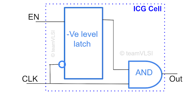
There are various ways to implement the clock gating techniques and there are many architectures of ICG cells also. Here the most common architecture is Latch-AND based ICG cell.
 |
| Figure-1: Latch-and based ICG Cell |
The function of ICG Cell:
As shown in the above figure it provides a glitch-free clock gated output. and passed the clock single only when the enable signal is high and stop the clock propagation when enable signal is low.
Why not only AND gate as a clock gating?
The issue with the AND gate as clock gating is, it can not provide a glitch-free output whereas a glitch-free clock wave is highly desired.
 |
| Figure-3: AND gate as a clock gater |
If there is a transition in clock enable signal when the clock signal is low, there is no effect on the gated clock. But if there is a transition in clock enable signal when the clock signal is high, there will be a glitch in the gated clock. To suppress such glitches, latch-and gate based ICG cell is preferred.
The placement of ICG cells will be discussed in the next article.
Thank you


Excellent content Rajesh...But I have one doubt...why do we use latch for ICG? why not a register?
ReplyDeleteHi Ram,
ReplyDeleteGood question
I have not discussed on this point in order to keep the article limited to only ICG cell.
I am adding the answer of your question in the bottom of article. :)
What happens if we use +ve edge triggered flop.
DeleteThere seems to be no issue as along as you meet the setup time requirement for en signal.
Although using -ve latch is more area and power efficient .
hi sir very small change should be made i think in this line "But if there is a transition in clock enable signal when the clock signal is low, there will be a glitch in the gated clock " the glitch will occer only when clock signal is high not at low for the case you taken thank you sir very nice artical
ReplyDeleteThanks a lot Dantu for your feedback.
DeleteSame has been corrected.
Keep suggesting!!!