04 August

Physical Design Interview Questions for 3 years experience , Question set - 8

Code: EXIM4Y062021PD


Experience level : 3 years
    1. Brief Introduction and major projects?
    2. Tell me the most challenging part of your recent project
    3. How does the lockup latch help to fix hold violations?
    4. If we add a lockup latch, it might violate the setup? How will we fix it further?
    5. How did you fix SigEM? What are patch wires?
    6. What CTS constraints have you used?
    7. How did you fix the setup violation?
    8. Apart from setup and hold, what other checks do we perform in timing signoff?
    9. What are the PV checks?
    10. What are the sanity checks we do before starting PnR?


    11. What are the reports of synthesis we check before PnR?
    12. What are the physical cells we have used in PD and what are the uses of all those?
    13. What is the latch-up issue and how well tap cells prevent latchup?
    14. What is the endCap cell and what is the purpose of using that?
    15. What is Dcap Cell and why do we use it?
    16. What is the antenna effect?
    17. What are the ways to fix the antenna effect?
    18. How do antenna diodes help to fix the antenna violations?
    19. If we have timing criticality and we can't use antenna diodes or floating gates, How can we fix the antenna?
    20. If antenna violation is already the highest metal layer and we can use higher metal for metal hopping, how will fix the antenna?
    21. How will you fix the antenna violations on via?
    22. What is a metal cut layer?
    23. What is the crosstalk delay?
    24. What is the crosstalk noise?


Physical Design Interview Questions : Question set -7


Code: CDN5Y062021PD


Experience level: 5 Years
For Application Engineer


  1. What are the major differences between 7nm and 12/14nm technology nodes?
  2. What are the new DRC rules in the 7nm technology node?
  3. What is the via-piller?
  4. What is double patterning?
  5. How many layers have double patterning in the 7nm node?
  6. How tool performs placement steps?
  7. Why do we perform scan chain reordering?
  8. What is scan mode, why do we need that?
  9. What is ECF (Early Clock Flow) flow?
  10. What are the benefits of ECF flow?


  11. Can you explain the CTS flow?
  12. What are the low power techniques used in data and clock paths?
  13. Where does the clock-gater use?
  14. Have you built a custom clock tree?
  15. What are the constraints you have given to the clock tree?
  16. How did you solve max_trans violations in the clock path?
  17. How to provide different clock tap points in H-Tree?
  18. How many clocks were there in your block?
  19. How were they related?
  20. How did you analyze the clock domain crossing paths?
  21. What is a lock-up latch and how does it helps in hold fixing?
  22. What was the target skew in your block?
  23. What value of skew you achieved?


08 July

Placement Steps in Physical Design

Placement is a very important stage of physical design where all the standard cells get placed inside the core boundary. Overall QoR of the design greatly depends on the fact that how well placement is done. You must have noticed that the placement stage takes quite a large runtime. Actually, the tool performs various steps in a sequence to complete the placement stage. In this article, we will try to understand what are the important steps and the order in which the EDA tools perform to complete the placement stage.

Placement is the process of placing the standard cells inside the core boundary in an optimal location. The tool tries to place the standard cell in such a way that the design should have minimal congestions and the best timing. Every PnR tool provides various commands/switches so that users can optimize the design in a better way in terms of timing, congestion, area, and power as per their requirements. Based on the preferences set by the user, the tool tray to place and optimize it for better QoR. Placement does not place only the standard cells present in the synthesized netlist but also places many physical only cells and adds buffers/inverters as per the requirement to meet the timings, DRV, and foundry requirements. Here are the basic steps which the tool performs during the placement and optimization stage.


placement steps:

  1. Pre Placement
  2. Initial Placement / Course Placement / Global Placement
  3. Legalization
  4. HFNS (Hign Fanout Net Synthesis)
  5. Iteration for Congestion, Timing, DRV, and Power Optimization
  6. Multibit flop conversion
  7. Timing optimization iterations
  8. Scan-Chain Reorder
  9. Tie Cell insertion
  10. Save Design


1. Pre Placement:


Figure-1: Pre-placement step

Before starting the actual placement of the standard cells present in the synthesized netlist, we need to place various physical only cells like end-cap cells, well-tap cells, IO buffers, antenna diodes, and spare cells. A typical view after preplacement has shown in figure-1. Why these cells are required to place and how do we place them has been discussed separately in this article. Here we will focus mainly on the placement steps of standard cells present in the synthesized netlist.

2. Initial Placement / Global Placement / Course Placement 


Figure-2: Global placement before legalization

Once the pre Placement stage has been completed, We can start the placement of standard cells but before that, we have to provide all the correct placement and optimization settings that we want to be applied while the tool does the placement and optimization. These settings could be like partial placement blockage or density screen setting, bound or region creation, cell/instance padding, path_groups and effort, enabling the early clock flow (ECF) in case of innovus, enabling the extreme flow, enabling the useful skew, global congestion effort, global timing effort, power effort, Multibit flop conversion and many more.

After providing all these placement settings we can call the placement command (place_opt_design in case of innovus). The tool first does the global placement in which the tool determines the approximate location of each cell according to the timing, congestion, and multi-voltage constraints (in the case of innovus Gigaplace engine is called in this step). Any pre-placed macros will work as a placement blockage. In this stage, the tool will not check any overlap of instances. A typical figure of global placement has shown in figure-2 where you can see that the standard cells are placed in an approximate location but without legalization. 


3. Legalization

In the global placement stage, the instances are left with overlap. In this step, the tool will move the instances in nearby places to overcome the overlap. To match the proper power pins like the vdd pin of a standard cell should be on the vdd rail and vss on vss rail and for that if the fliping of instance is required tool also do the flipping. This process is called legalization. After this step, every instance should be placed in a legal location and there should be no overlaps. This step is also called refine placement.

4. HFNS (Hign Fanout Net Synthesis)

Initially, there are some nets which have very high numbers of fanout. We have a constraint of maximum fanout, so we need to distribute the sinks on nets to different drivers. The process of adding buffers and splitting the fanout is called high fanout net synthesis (HFNS). So In this step, all high fanout nets get synthesized.

5. Iteration for Congestion, Timing, DRV, and Power Optimization

In this step tool first, do an early global route and estimate the routing overflow/congestions in the design. The tool tries to initially minimize the congestion in this stage. Next, the tool starts the RC extraction to calculate the delay for setup analysis. The tool tries to minimize the setup WNS and TNS in this step. Similarly, the tool also tries to minimize the DRV and Power in this stage.

6. Multibit flop conversion

If the user enables the multi-bit flip flop conversion in the flow then the tool will first check the available multibit flops in the library. (You can read more about multi-bit cell here) The tool considers the criticality of timing associated with a single bit of flop and the user constraint set for multi-bit conversion and based on the constraints the tool converts the single-bit flop into multibit flops.

7. Timing optimization iterations

This is a long step in which the tool tries to minimize the WNS and TNS of each path group in various iterations. There are several iterations required to get a minimum WNS and TNS depending upon the effort set and initial WNS number. In case the result is not good after this stage, we can further run incremental optimization for timing. Similarly, for congetion, we can run congestion repair followed by incremental optimization to get a better result. But these additional steps will increse the run time.

8. Scan-Chain Reorder


Figure-3: Scan Chain before placement

Scan chain stitching has been done arbitrarily in synthesis. After placement and optimization, we have a location for each scan flops so it needs to be reordered for better routability. The tool performs a reordering of the scan chain in this step which is good for both timing and congestions. 

Figure-4: Scan chain after placement

Figure-5: Scan Chain after Scan chain reodrder


9. Tie Cell insertion

There are some unused inputs of logic gates in the netlist which is tied to either vdd or vss. We can not leave any inputs of the standard cell as floating, it must be tied either vdd or vss. Connecting an input of logic cell that is the gate of a transistor directly to vdd or vss is not recommended and for that, we have tie high and tie low cells in the library. (You may watch this video on tie cells for more details). So In this step tool places tie high and tie low cells which is basically a single output logic cell, and it connects the input of the logic gate which needs to connect vdd or vss respectively. 

10. Save Design

Finally, we save the database and we will use this database in the next stage, that is in the clock tree synthesis.

28 June

Clock Tree Constraints in VLSI | ccopt file in Physical Design | CTS Constraints

Clock tree synthesis is a process of building and optimizing the clock tree in such a way that the clock gets distributed evenly and every sequential element gets the clock within a target global skew limit. To build the clock tree we have to provide certain constraints as input to the APR tool, which commonly known as clock constraints, and in the case of the Innovus tool, this constraint file is popularly known as ccopt file.

In this article, we will learn some important clock tree constraints which are commonly used in every design and their actual meaning that why those constraints provided. Now a day it's very common that if you are going to appear in an interview in physical design and your experience is in the bracket of 0-5Y, you have to face the question related to clock tree constraints in your interview.


clocks tree constraints:

  1. Clock tree cell list
  2. Preferred clock tree routing layers and Non-Default Rules (NDR)
  3. Target Skew
  4. Target Maximum Transition
  5. Target Maximum Capacitance
  6. Maximum Fanout
  7. Cell Density
  8. Cell Halo 

1. Clock tree cell list

We use clock inverters and clock buffers in the clock tree building. Sometimes we use only clock inverters and not clock buffers. We also use clock gating cells in the clock tree. so we have to provide the list of cells that we want to use in the clock tree.

set_ccopt_property inverter_cells {}
set_ccopt_property buffer_cells {}
set_ccopt_property clock_gating_cells {}
set_ccopt_property logic_cells {}

2. Preferred clock tree routing layers and Non-Default Rules (NDR)

We need to provide the top and bottom preferred routing layer for clock tree nets. We generally define here trunk and leaf net. the net which connects the clock to the sequential element's clock pin is called the leaf net and the net which delivers the clock to the leaf net is called trunk net.

set_ccopt_property  -name trunckRoute -top_preferred_layer <> -bottom_preferred_layer <> -preferred_routing_layer_effort high -non_default_rule 2w2s

set_ccopt_property  -name leafRoute -top_preferred_layer <> -bottom_preferred_layer <> -preferred_routing_layer_effort high -non_default_rule 1w2s

3. Target skew

Skew balancing is one of the challenges in clock tree optimization. We provide a target skew as a clock tree constraint. PnR tool will try to balance the skew within the given limit of skew.

set_ccopt_property -target_skew <> 

4. Target Maximum Transition

We provide a max_trans limit for clock nets in the clock tree constraint. The tool will try to meet the max_trans limit.

set_ccopt_property -target_max_trans <> 

5. Target Maximum Capacitance

We provide a max_cap limit for clock nets in the clock tree constraint. The tool will try to distribute the load capacitance and try to meet the max_cap limit.

set_ccopt_property -target_max_capacitance <> 

6. Maximum fanout

We limit the maximum fanout of any instance in the clock tree through this constraint. Tool will try to build the clock tree by following this limit. 

set_ccopt_property -max_fanout <> 

7. Cell Density

A maximum cell density limit is mandatory for the clock tree instances.

set_ccopt_property -cell_density <>

8. Cell Halo

We need to provide a halo around the clock tree instance to avoid a denser placement which may cause IR / Crosstalk issue. So we provide halo constraints in the x and y direction over the cells.

set_ccopt_property -cell_halo_x <>  
set_ccopt_property -cell_halo_y <>  


These are the main constraint which we provide before the clock tree building. There are some more constraints but the main constraints are explained in the above sections. The following image summarizes the clock tree constraints.

CTS Constraints


Thank you! Any suggestions are welcomed in the comment section.

05 June

Installation of Synopsys EDA tools

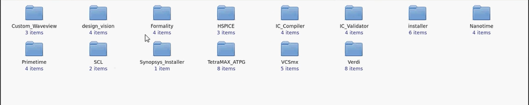
Most of the EDA tools used in the VLSI Industry are designed for use in UNIX operating system. These tools must require licenses to work which can be purchased from EDA Companies or a company that is authorized for sales and supports. Synopsys tools can be purchased either from www.synopsys.com or from authorized sales and support partner www.eigen.in (in India). 

Once you buy the tools, they provide login credentials on their website. Using the login credential the licenses and tools can be downloaded to your local machine/server. We can also update the licenses whenever it gets expired and we can also download the latest release of any tools from the website using the login credential. For Synopsys tools, we need to login into their official website https://solvnet.synopsys.com to download the tools and licenses.

Generally, EDA companies provide support to install the tools and help in case of any issue, but it's better to know the installation process of tools and basic debugging to manage the tools in our own hands. The following section is going to describe how to download and install the Synopsys tools in your local machine/server.

Step-1: Download the synopsys installer, SCL and tools setup files

Go to https://solvnet.synopsys.com and login with your login credentials.

Solvenet Login

After login, you need to download:

  1. Synopsys Installer (An application which provinde nice gui interface to install the tools)
  2. SCL (Synopsys Common Licensing)
  3. All the EDA tools which you have license and want to install.
  4. Synopsys license (Incase it is not set already)


Step-2: Launch the synopsys installer GUI

Step-2.1: Open the terminal with root prevelage and go to the directory where synopsys installer is downloaded.


Step-2.2: Provide the execute permission to the synopsysInstaller.

chmod 755 synopsysInstaller_V3.2.run

Step-2.3: Run the following commands to unpack the installer ( -d switch is for creating a directory)

 ./synopsysInstaller_V3.2.run -d installer

Step-2.4: Go to installer directory created in above step and if you see the contents, it will look like. 

cd installer

ls installer 


Step-2.5: Now we have to launch the installer in GUI mode by following command.

./installer -gui 

Step-3: Provide the source location (installation setup directory) and destination location (directory where you want to install the tool)

Step-3.1: After above step a GUI will be opened up. Now when we click to start, it will ask to site ID which is provided by synopsys when you purchase the tool.


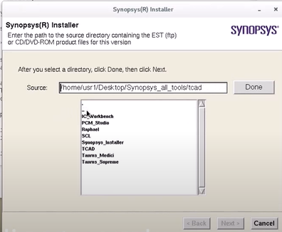
Step-3.2: Next we need to provide the source location where the tools is kept which we want to install.


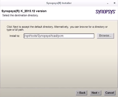
Step-3.3: Next we need to provide the destination location where we want to install the tool.


Step-3.4: Next we need to accept and proceed, after that installation will be started.


 In the same way, we can install all the tools.Once we done with installation we need to configure the license and set a path of all the tools in form of a bashrc/cshrc file. That will be explained in seprate article.


Thanks


29 May

Temperature Inversion in VLSI

If a simple question comes before you that "What will impact on the delay of a standard cell if temperature varies? " Are you going to answer straightforward the delay of the cell will increase with temperature OR The delay of the cell will decrease with temperature? If you are going with either of the above answers, Then you need to spare some moment in this article and understand the concept of Temperature Inversion.


Figure-1: Trend of cell delay with temperature


What is temperature inversion?

In general, as temperature increases, the delay of standard cells increases because of mobility degradation at higher temperatures. But in lower technology nodes the impact of temperature on the delay of the cell is inverse. In lower nodes, the delay of the cell decreases with an increase in temperature. So in the lower technology node, the effect of temperature on the delay of the cell is inverted and this effect is called the temperature inversion. The main reason behind this inversion is in the lower technology node, the effect of the threshold voltage is dominating over the mobility. 

So an appropriate answer to the above question could be we should answer this question with respect to the technology node. One can say that at the lower technology nodes as temperature increases the delay of cell decreases. Here lower technology node means the technology node below 65nm. Why part of this question is important, but we should wait if it is asked further. In the next part, we will learn why temperature inversion occurs.

Figure-2: Temperature inversion

The following section will explain in detail of factors affecting the delay of cells and their variation.


Reason for temperature inversion

The delay of a cell is simply the time required to charge/discharge the load capacitance. The charging and discharging time of the load capacitor depends on the drain current. If the drain current is high, it will take a lesser time to charge/discharge the load capacitor and so delay will be lesser and vice-versa. Now let's see the dependency of drain current Id.

The saturation current of MOSFET is,

The drain current Id is directly proportional to the mobility of charge carriers. So as the temperature increases, the lattice scattering increases, and ultimately the mobility of the charge carrier decreases which leads to the decrease in drain current Id and so it increases in the delay of the cell. 

Now let's come to the second important factor, the term (Vgs - Vt) in the above equation is called overdrive voltage. There is a variation in threshold voltage with temperature as per the following equation,

As temperature increases, the threshold voltage decrease, and overdrive voltage increases. This overdrive voltage is more dominating in the lower technology node because in the lower technology node the Vgs and Vt are more closers and so a slight change in Vt will have more impact on overdrive voltage. But in a higher technology node since Vgs is much larger than Vt so a slight change in Vt not causes much change in overdrive voltage. Again the Id is proportional to the squire of overdrive voltage. So changes in overdrive voltage are further amplified and it is dominating over the mobility in lower technology node. 


In a nutshell, In a lower technology node, as temperature increases the threshold voltage decreases so overdrive voltage and drain current increase which leads decrease in cell delay. Here overdrive voltage is dominating over the mobility factor. But in higher technology nodes, overdrive voltage is not much dominating, and delay of the cell varies as per variation in carrier mobility and we have discussed as temperature increases mobility decreases and so drain current decreases which lead increase in cell delay. 

So There are two major factors that drive the variation in cell delay, mobility and overdrive voltage. In lower technology nodes overdrive voltage is more dominating which causes the temperature inversion effect.

Thank you.